
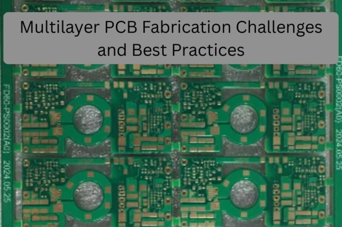
The PCBs Multilayer printed circuit boards (PCBs) occupy the core of the current realization of electronics, including smartphones and routers, industrial controls, and car systems. With the dimensions of designs reducing and functionality growing, the use of many copper and dielectric layers stacked becomes the sole viable method of routing dense and high speed signals with a compact size. This sophistication however does not come without special manufacturing challenges. These issues, along with how the experienced partners deal with them, have to be known before you place your initial order of multilayer pcb fabrication.
The Multilayer PCBs are a difficult challenge
Multilayer PCBs demand much better process control and equipment capability compared with basic two layers boards. The matter is that during lamination all the internal copper layers, and dielectric prepregs should all be in line; any tiny misregistration may result into shorting, voiding, or impedance variations. Bow and twist, copper thickness variation, delamination, and uptake of moisture are also considered to be increasing with the increases of the number of layers, which may result in long-run reliability breakdowns.
Another point of pressure is drilling. Blind and buried vias, back-drilled holes and microvias require high precision of micrometers to strike small pads without inner connection destruction. Added complexity- Thermal and electrical performance Performance at high frequencies Thermal and electrical performance may result in a hot spot, signal integrity problems, or EMI due to poor stack-up choices. These facts are the reason why most designers are choosing custom pcb fabrication services with complex builds, over general low cost.
Ordinary: Problems and Solutions
The following are some of the failure modes recurring in multilayer production. Misregistration of layers i.e. when the inner images move during the lamination or drilling process, the vias and pads will be misaligned. Front line fabs can counter this by X-ray registration system, controlled lamination cycles and symmetrical stack-ups which equalize mechanical stress. The other common problem is copper thickness variation, which is reduced by means of a well-controlled plating chemistry and optimization of panel layouts.
Delamination and No. V. may be dated on bad material selection, moisture, or improper lamination pressure and temperature. Typical countermeasures include the selection of low-hygroscopic laminates, pre-baking cores and prepregs as well as IPC-qualified material. When drilling is involved such defects as smear, mis-drilled vias, and stuck drill bits are reduced to sharp tooling, optimized feeds and speeds, and post-drill desmear/cleanup. Signal integrity issues (crosstalk, reflections or excessive losses) When signal integrity issues become apparent (placing signal and continuous ground planes in contact), the fix has been found in redesigning the stack-up such that the signal and ground traces are stacked adjacent to continuous ground systems and by regulating trace impedance (might be 50 ohms).
By collaborating with a well established pcb fabrication manufacturer with a well developed troubleshooting playbooks of these issues, your learning curve is seriously reduced.
Best Practices of Reliable multilayer boards design
Good production of fabrications begins with good design. Researchers suggest that a carefully thought-out stack-up should be started with: symmetrical around the centre line, and the power and ground planes should be placed to offer high-speed nets good return paths and controlled impedance. Storing high-speed or sensitive signals on the inner layer where there is a sandwich of reference planes can be used to reduce EMI and enhance signal integrity.
Via strategy matters too. The number of unnecessary via types should be minimized; only blind and buried via should be used when the density requires them since they complicate and add to the fabrication costs. Be sure (through aspect ratios (board thickness to drill diameter)) are within the recommended aspect ratios of your fab to prevent plating problems. In delivering power, reserve and encircle the amplified copper planes very well and add numerous stitching vias to reduce impedance and dissipate heat.


Special attention should be paid to the clear communication with your fab: better known fabrication notes, impedance goals, tolerances, and desired materials should be included in your drawings and readme files. With the custom pcb fabrication you are using, take advantage of their feedback on DFM (Design for Manufacturability), most of the problems such as minimum trace/space, copper balancing etc can be sorted out prior to production even in the early days as well.
Selecting the appropriate manufacturing ally
Multilayer work is a demanding task; hence, your project might make or break it depending on the choice of vendors. An area and competent pcb fabrication manufacturer must show:
- Existing HDI stack-ups HDI stack-ups of high layer counts.
- Availability of materials with high grade standards (FR, high Tg, low-loss, PTFE, etc prices) based on IPC and industry standards.
- High- technologies of imaging, lamination and drilling (X-ray registration and laser drilling).
- Strong in-process control and end test (AOI, impedance testing, micro-section analysis).
The assembly providers, which also provide assembly – actual custom pcb fabrication services, are able to guide you through the entire cycle of bare board to populated PCB identifying potential issues in solderability or components before it is late it ispopulated. To engineers designing complicated prototypes or getting ready to engage in mass production, it is easier to have both the fabrication and assembly under a single roof, logistics is easy and accountability is enhanced.
Quality and Process Best practices
Both designers and the manufacturers need to observe disciplined practices in order to achieve similar results with multilayer pcb fabrication. On fab side, resin starvation and voids are eliminated by a strict control of lamination temperature profiles, pressure, and ramp rates. Pre-baking of requirements minimizes defects that are caused by moisture and frequent calibration of the drilling and imaging systems maintains spec-registered.