

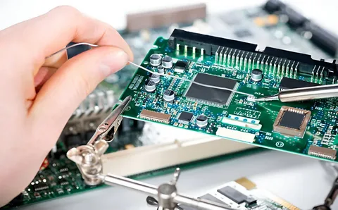
Surface Mount Technology (SMT) has revolutionized electronic manufacturing by enabling high-density, compact, and efficient circuit boards. However, like any manufacturing process, SMT PCB assembly is not immune to defects. These issues can arise from various stages—design, component placement, soldering, or even handling. Identifying and troubleshooting these defects is crucial for ensuring quality, reliability, and long-term performance of electronic devices.
- 1. Solder Bridging
- 2. Tombstoning
- 3. Solder Balling
- 4. Open Circuits
- 5. Component Misalignment
- 6. Insufficient or Excessive Solder
- 7. Voiding
- 8. Delamination
- What it is:Layers of the PCB separate due to heat or moisture during the reflow process.
- Causes:
- Troubleshooting:
- Best Practices for Minimizing Defects
- Conclusion
This article will explore the most common defects in SMT PCB assembly, their causes, and practical troubleshooting methods.
1. Solder Bridging
What it is:
Solder bridging occurs when excess solder creates an unintended electrical connection between two or more adjacent pads or component leads. This can result in short circuits, overheating, and device failure.
Causes:
- Excessive solder paste application
- Incorrect stencil design or thickness
- Misalignment of components
- Inconsistent reflow oven temperature profile
Troubleshooting:
- Optimize stencil aperture size to control solder paste volume.
- Use high-precision placement machines to avoid misalignment.
- Calibrate reflow profiles to ensure proper melting without excess flow.
- Regularly inspect solder paste printing for uniformity.
2. Tombstoning
What it is:
Tombstoning, or the “Manhattan effect,” occurs when one end of a small passive component (like a resistor or capacitor) lifts off the pad during reflow, standing upright instead of lying flat.
Causes:
- Uneven heating during reflow
- Imbalanced solder paste deposition
- Incorrect pad design
- Component size mismatched to pads
Troubleshooting:
- Adjust the thermal profile to ensure even heat distribution.
- Use symmetrical pad designs with equal solder volumes.
- Maintain consistent paste thickness.
- Check for correct component size and placement accuracy.
3. Solder Balling
What it is:
Small spheres of solder that adhere to the PCB surface outside the intended solder joint area.
Causes:
- Excessive flux in the solder paste
- Rapid heating during reflow
- Contaminated PCB surface
- Poor paste quality or storage
Troubleshooting:
- Store solder paste under recommended conditions.
- Clean PCB surfaces thoroughly before assembly.
- Gradually increase heat in the preheat stage to reduce splattering.
- Select high-quality solder paste with controlled flux content.
4. Open Circuits
What it is:
An open circuit defect happens when the solder fails to create a complete electrical connection between the component lead and the pad.
Causes:
- Insufficient solder paste application
- Component misplacement
- Cold solder joints due to improper reflow temperature
- Oxidized component leads or PCB pads
Troubleshooting:
- Ensure accurate solder paste deposition using well-maintained stencils.
- Verify placement accuracy through automated optical inspection (AOI).
- Clean and deoxidize surfaces before soldering.
- Adjust reflow temperature to achieve complete solder wetting.
5. Component Misalignment
What it is:
Components are placed outside their designated positions, which can lead to poor connections or mechanical stress.
Causes:
- Inaccurate pick-and-place machine calibration
- Vibrations during placement
- Warped PCBs causing uneven surfaces
Troubleshooting:
- Calibrate and maintain placement equipment regularly.
- Use fiducial marks for machine alignment.
- Ensure PCBs are flat and within tolerance before placement.
6. Insufficient or Excessive Solder
What it is:
Too little solder can cause weak joints, while too much solder can result in bridging or reduced mechanical stability.


Causes:
- Incorrect stencil thickness or aperture design
- Variations in paste viscosity
- Operator error during manual soldering
Troubleshooting:
- Match stencil thickness to component and pad requirements.
- Monitor solder paste rheology and replace if degraded.
- Train operators on correct soldering techniques.
7. Voiding
What it is:
Voids are trapped air or gas pockets within a solder joint, weakening its mechanical and thermal properties.
Causes:
- Poor paste printing or placement
- Excessive flux
- Rapid heating during reflow
Troubleshooting:
- Optimize reflow profile to allow gas escape before full solidification.
- Control flux content in solder paste.
- Improve paste printing for uniform coverage.
8. Delamination
What it is:Layers of the PCB separate due to heat or moisture during the reflow process.
Causes:
- Moisture absorption in PCB material
- Excessive reflow temperature
- Poor PCB manufacturing quality
Troubleshooting:
- Bake PCBs before assembly to remove moisture.
- Use high-quality boards with proper lamination.
- Monitor oven settings to prevent overheating.
Best Practices for Minimizing Defects
- Pre-Assembly Checks: Inspect components, stencils, and boards before production.
- Regular Equipment Calibration: Maintain placement, printing, and reflow equipment.
- Use of Automated Inspection: Employ AOI and X-ray inspection to detect defects early.
- Training Operators: Skilled staff can identify issues before they escalate.
- Environmental Control: Maintain humidity and temperature in the assembly area.
Conclusion
Defects in SMT PCB assembly can result in significant losses in time, cost, and reputation if not addressed promptly. By understanding common issues, their root causes, and implementing targeted troubleshooting strategies, manufacturers can maintain high production quality and reliability. Proactive maintenance, process optimization, and a strong focus on quality control are the keys to producing defect-free circuit boards.