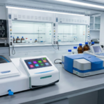

In the world of modern electronics, devices are becoming increasingly compact, powerful, and feature-rich. Meeting these demands requires printed circuit boards that can handle high component density while maintaining top-tier performance. This is where high density interconnect PCB technology comes into play. HDI PCBs allow engineers to create more complex, high-performance designs in smaller spaces, making them essential for advanced electronics in consumer, medical, industrial, and aerospace applications.
High density interconnect PCBs stand out because they enable smaller, lighter devices without compromising reliability or functionality. By incorporating features like microvias, blind and buried vias, and ultra-fine traces, these boards maximize circuit density and improve electrical performance. For any electronics project where space, speed, and precision are critical, HDI PCBs offer the ideal solution.
Understanding High Density Interconnect PCBs
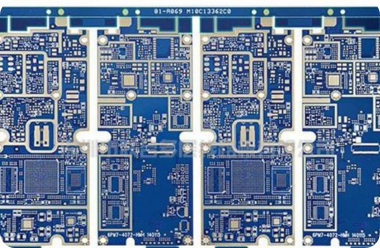
HDI PCBs are designed to allow more interconnections per unit area than conventional boards. This is achieved through advanced manufacturing techniques that create fine lines, small spaces, and multi-layered structures. Microvias—tiny holes that connect different layers of the board—are a hallmark of HDI technology, allowing circuits to be tightly packed without sacrificing performance.
Applications of high density interconnect PCBs are widespread, including:
- Smart Devices – Smartphones, tablets, and wearable electronics benefit from compact, high-performance circuit designs.
- Medical Electronics – Portable diagnostic equipment and wearable monitors require dense circuits in tight spaces.
- Industrial and Automotive Electronics – HDI PCBs allow advanced sensors and control modules to fit into compact mechanical assemblies.
- Telecommunications & Networking – High-speed networking equipment relies on HDI boards to maintain signal integrity at higher densities.
By enabling engineers to integrate more functionality into smaller devices, HDI PCBs make modern electronics more efficient, reliable, and innovative.
Key Benefits of HDI PCB Technology
Choosing high density interconnect PCBs provides several advantages:
- Miniaturization – HDI technology supports smaller, lighter, and more compact devices without sacrificing functionality.
- Enhanced Signal Integrity – Shorter electrical paths reduce signal delay, crosstalk, and resistance, improving overall performance.
- Design Flexibility – Multi-layer HDI boards allow more complex circuit layouts and innovative component placement.
- Improved Reliability – By reducing the number of interconnections and solder joints, HDI PCBs minimize potential points of failure.
- Faster Development Cycles – Engineers can rapidly prototype and test high-density designs, accelerating time-to-market.
These benefits make HDI PCBs a cornerstone for developing next-generation electronics that require high performance in small form factors.
How FastTurn PCB Simplifies HDI PCB Manufacturing
FastTurn PCB specializes in delivering high-quality HDI PCB solutions that balance precision, performance, and speed. Their advanced manufacturing capabilities and skilled team ensure that even the most complex designs are produced reliably and efficiently.


FastTurn PCB offers:
- Advanced Fabrication Technology – Expertise in microvias, high layer counts, and fine line spacing ensures precision in every board.
- Design Collaboration – Engineers can work with FastTurn PCB to optimize layouts, select materials, and prevent manufacturability issues.
- Rapid Turnaround – From prototype to production, FastTurn PCB accelerates timelines while maintaining high-quality standards.
- Customized HDI Solutions – Boards are tailored to project requirements, including thickness, layer count, and via types.
By leveraging FastTurn PCB’s HDI manufacturing capabilities, engineers can focus on innovation while leaving complex fabrication challenges to the experts.
Applications Across Industries
HDI PCBs are critical for industries where performance, reliability, and compact design are essential:
- Consumer Electronics – Smartphones, tablets, and wearable devices demand miniaturized, high-density circuits.
- Medical Devices – Compact, reliable boards power portable diagnostic tools, monitors, and implants.
- Aerospace & Defense – Lightweight, high-performance HDI boards are ideal for navigation, communication, and control systems.
- Industrial Automation – Machinery and robotics benefit from compact, high-density circuits for efficient operation.
With HDI technology, engineers can achieve greater functionality, better electrical performance, and more innovative device designs.
Conclusion
High density interconnect PCBs are transforming the way modern electronics are designed and manufactured. By enabling compact, reliable, and high-performance circuits, high density interconnect PCB solutions allow engineers to develop next-generation devices efficiently and effectively.
For companies and designers seeking precision, speed, and innovation in HDI PCB manufacturing, FastTurn PCB is the trusted partner. Their expertise, advanced fabrication techniques, and commitment to quality ensure that your electronics projects are executed flawlessly, from prototype to production. With FastTurn PCB, engineers gain the tools and support needed to bring high-performance, high-density electronics to life.