

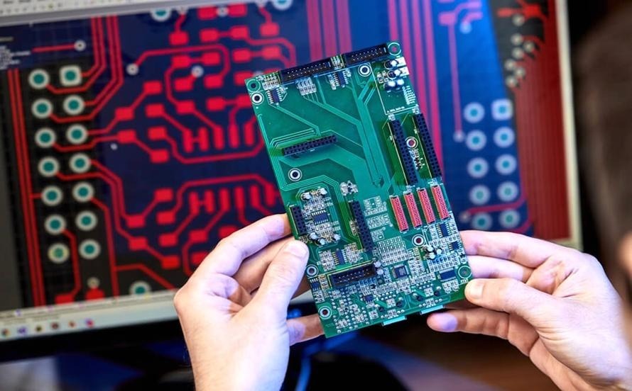
In the modern electronics industry, where data transmission speeds continue to rise and signal integrity is paramount, the Impedance Control PCB plays a critical role. These specialised circuit boards are designed to maintain consistent electrical impedance across conductive traces, ensuring that high-frequency signals travel smoothly without distortion or loss. Whether used in telecommunications, computing, automotive systems, or aerospace technologies, impedance-controlled boards are essential for reliable high-speed performance.
What Is an Impedance Control PCB?
An Impedance Control PCB is a printed circuit board engineered to maintain specific impedance values for signal traces. Impedance is the opposition a circuit presents to the flow of alternating current, and it’s measured in ohms (Ω). In high-speed digital and RF (radio frequency) circuits, maintaining a consistent impedance along signal paths prevents reflection, signal degradation, and data loss.
When the impedance of a trace doesn’t match the impedance of the source or the load, part of the signal is reflected back. This reflection leads to interference and reduced performance—issues that are particularly problematic in applications like HDMI, USB, RF transmission, and Ethernet. Therefore, controlling impedance during PCB design and fabrication is crucial to ensure the board functions as intended.
Why Impedance Control Matters
As signal frequencies increase, the behaviour of electrical traces starts to resemble that of transmission lines rather than simple conductors. This means the physical dimensions of the trace, the dielectric material used, and even the layer stack-up directly affect impedance.
The Impedance Control PCB ensures that:
- Signal reflections are minimised, maintaining clean signal transmission.
- Crosstalk between adjacent traces is reduced.
- Devices operate efficiently within their required bandwidth.
- System performance remains stable under high-frequency conditions.
In short, precise impedance control is vital for maintaining the integrity of complex digital and RF systems.
Key Factors Affecting PCB Impedance
Creating an Impedance Control PCB requires a deep understanding of several interrelated design and material factors:
1. Trace Width and Thickness – The width and thickness of copper traces are major determinants of impedance. Wider traces reduce impedance, while narrower ones increase it.


2. Dielectric Constant (Dk) – The dielectric material separating the trace from the ground plane affects the board’s electrical properties. A lower Dk results in higher signal speed but lower impedance.
3. Dielectric Thickness – The distance between the signal trace and the reference plane impacts impedance. Thicker dielectric layers increase impedance, while thinner layers lower it.
4. Copper Weight – The thickness of copper used in the PCB also affects the impedance values. Standard copper thicknesses like 1oz or 2oz are commonly used, but variations must be carefully calculated.
5. Trace Spacing and Geometry – The layout, especially for differential pairs, influences impedance matching. Differential traces must be routed with consistent spacing to achieve the desired impedance value (typically 90Ω for differential signals).
6. Manufacturing Tolerances – Even minor deviations during PCB fabrication can alter impedance values. That’s why choosing an experienced manufacturer with advanced equipment is essential.
Types of Impedance Control
There are generally three categories of impedance control in PCB design:
1. Single-Ended Impedance – Used for a single trace carrying a signal referenced to ground, commonly found in USB or RF applications.
2. Differential Impedance – Used for pairs of traces carrying complementary signals (positive and negative). Differential signalling is common in Ethernet, HDMI, and LVDS circuits, where both traces must maintain the same impedance and spacing.
3. Coplanar Impedance – Involves traces surrounded by ground planes on the same layer, offering additional control and isolation for RF applications.
Designing an Impedance Control PCB
Designing an Impedance Control PCB requires the integration of electrical and mechanical engineering expertise. The process begins with simulation and impedance calculation using tools such as Polar SI8000, HyperLynx, or Altium Designer’s field solver.
Once the ideal trace dimensions and layer stack-up are defined, detailed fabrication notes are included in the Gerber files, specifying target impedance values and acceptable tolerance ranges (typically ±10%). During production, the manufacturer measures and verifies impedance through test coupons—small test sections fabricated alongside the main PCB to ensure the final board meets design requirements.
Applications of Impedance Control PCBs
Because of their stability and accuracy in high-speed applications, Impedance Control PCBs are widely used in:
- Telecommunication equipment such as routers, 5G base stations, and switches
- Consumer electronics, including laptops, smartphones, and smart TVs
- Automotive electronics, especially in advanced driver-assistance systems (ADAS)
- Aerospace and defence systems where reliability and signal integrity are critical
- Medical devices that depend on precise data transmission, like diagnostic imaging equipment
Manufacturing Challenges and Quality Assurance
Producing an Impedance Control PCB is more complex than standard board fabrication. Manufacturers must carefully manage every variable—material quality, layer registration, etching precision, and plating consistency.
Advanced manufacturing techniques, such as laser-controlled depth drilling and automated optical inspection (AOI), are often employed to ensure compliance with tight impedance tolerances. Moreover, environmental factors like humidity and temperature must be regulated during production to avoid variations in dielectric properties.
A top-quality PCB manufacturer will also perform time-domain reflectometry (TDR) testing to confirm that each batch meets the specified impedance requirements.
Conclusion
The Impedance Control PCB is an indispensable component in today’s high-speed electronics. It ensures that signals are transmitted accurately and efficiently, supporting the performance and reliability demanded by cutting-edge technology. From telecommunications to aerospace systems, impedance-controlled boards underpin the success of complex electronic designs.
If you’re looking for consistent quality and precision in high-frequency PCB production, partnering with a trusted China PCB Manufacturer is a smart choice. China’s leading PCB manufacturers combine advanced fabrication capabilities with rigorous testing to deliver reliable, high-performance boards that meet exact impedance specifications. By choosing an experienced Chinese partner, you can ensure your PCBs are built to the highest international standards—empowering your innovations with stability, speed, and signal integrity.