

Portable electronic devices have become indispensable in our daily lives, yet power drain remains their most persistent challenge. When batteries deplete rapidly, user experience suffers dramatically, leading to frequent charging cycles and reduced device longevity. The quest for extended battery life has driven engineers to explore innovative solutions that balance performance with energy conservation. Among the arsenal of components available, the 555 IC chip stands out as a surprisingly versatile and cost-effective tool for improving power efficiency in portable applications. While often overlooked in favor of modern integrated solutions, this classic timer IC offers unique advantages for developers seeking practical power management strategies. This article examines how the 555 IC chip compares with advanced alternatives like the IT8502E KXS and other specialized power management ICs, providing developers with clear selection criteria based on their specific requirements. We’ll explore actionable design approaches for multi-channel power management systems, demonstrating how both traditional and contemporary ICs can be leveraged to maximize battery performance while maintaining compact form factors essential for portable devices.
- Understanding the 555 IC Chip in Modern Power Management
- Comparing Power Management ICs: 555 Chip vs. IT8502E KXS and Multi-Channel Solutions
- Practical Solutions for Selecting and Implementing Efficient Power Management
- Step-by-Step Guide to Selecting Suitable Power Management ICs
- Implementing Multi-Channel Power Management with the 555 IC
- Optimization Techniques for Maximum Power Efficiency
- Case Studies and Best Practices in Portable Device Design
- Strategic Power Management Implementation for Portable Devices
Understanding the 555 IC Chip in Modern Power Management
The 555 timer IC, introduced in 1972, remains one of the most widely used integrated circuits in electronics due to its remarkable versatility and reliability. At its core, this chip functions as a precision timing device capable of generating accurate time delays and oscillations, making it invaluable for power regulation tasks in portable devices. Its ability to operate across a wide voltage range while consuming minimal quiescent current positions it as a practical solution for battery-powered applications where efficiency matters.
In power management contexts, the 555 IC serves multiple functions beyond simple timing. It can regulate voltage levels through pulse-width modulation, control switching regulators, and manage power sequencing in compact circuits. The chip’s low component count requirements translate to reduced board space and lower overall system costs, critical factors in portable device design. While modern specialized power management ICs offer integrated features, the 555 maintains relevance through its adaptability—engineers can configure it for specific power management tasks without the constraints of fixed functionality found in dedicated solutions.
Core Principles and Applications
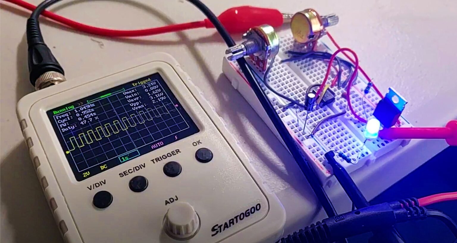
The 555 IC operates in two primary modes that directly benefit power efficiency. In astable mode, it generates continuous square wave pulses with adjustable duty cycles, enabling efficient switching power supplies that convert battery voltage to required levels with minimal energy loss. By varying the timing resistors and capacitors, designers can fine-tune switching frequencies to match load requirements precisely. In monostable mode, the chip produces single timed pulses ideal for controlling power-on sequences or implementing sleep modes that dramatically reduce standby current consumption. A simple circuit using the 555 as a voltage regulator controller requires just a handful of external components—two resistors, two capacitors, and a transistor—making it exceptionally suitable for space-constrained portable designs where every millimeter counts and cost sensitivity drives component selection.
Comparing Power Management ICs: 555 Chip vs. IT8502E KXS and Multi-Channel Solutions
Power management ICs span a broad spectrum, from simple discrete solutions to highly integrated system-on-chip designs tailored for specific applications. In portable electronics, the choice between these options hinges on factors like power density requirements, feature integration needs, and development constraints. The 555 IC represents the minimalist approach—offering fundamental timing and switching control with maximum design flexibility but requiring external components to build complete power systems. This contrasts sharply with modern integrated solutions that pack voltage regulators, sequencing logic, and protection circuits into single packages, reducing external component count at the cost of design adaptability.
IT8502E KXS for Advanced Multi-Channel Power Management
The IT8502E KXS exemplifies contemporary power management philosophy, integrating multiple voltage rails, programmable sequencing, and monitoring capabilities within a compact footprint. This IC manages several power channels simultaneously with independent voltage control, eliminating the need for multiple discrete regulators that would otherwise consume board space and increase complexity. Its built-in protection features—overcurrent detection, thermal shutdown, and soft-start functionality—provide robust operation without additional external circuitry. For developers building sophisticated portable devices like tablets or medical instruments requiring precise voltage regulation across multiple subsystems, such integration streamlines design and improves reliability. However, this integration comes with trade-offs: higher unit costs, limited configurability once specified, and steeper learning curves compared to the straightforward 555 IC approach that allows iterative prototyping with basic components.
Low-Power IC Strategies for Portable Devices
Achieving extended battery runtime demands careful attention to quiescent current—the power consumed by management circuitry itself when loads are inactive. Low-power ICs minimize this overhead through advanced process technologies and intelligent shutdown modes. The 555 IC, particularly CMOS variants, draws microamperes in standby, making it viable for intermittent operation scenarios like periodic sensor polling. Specialized low-power ICs push this further with nanoampere quiescent currents and dynamic power scaling that adjusts management overhead based on load conditions. The strategic choice involves matching IC characteristics to usage patterns: devices with constant background activity benefit from ultra-low quiescent current ICs, while those with burst operation modes can leverage the 555’s simplicity for cost-effective intermittent power control without sacrificing overall efficiency in real-world use.
Practical Solutions for Selecting and Implementing Efficient Power Management
Selecting the right power management IC for a portable device requires balancing technical performance against practical constraints that define project success. Developers must evaluate power efficiency metrics, physical dimensions, thermal characteristics, and budget limitations while ensuring compatibility with existing system architectures. The decision between using a 555 IC chip or advanced solutions like the IT8502E KXS fundamentally depends on application complexity and resource availability. Simple devices with single voltage rails and relaxed regulation tolerances benefit from the 555’s straightforward implementation, requiring minimal external components and offering rapid prototyping cycles. Conversely, multi-functional portables demanding synchronized power sequencing across multiple subsystems justify the investment in integrated solutions that consolidate regulation, monitoring, and protection features.


Step-by-Step Guide to Selecting Suitable Power Management ICs
Begin by quantifying power requirements: calculate total current draw for each voltage rail, peak transient demands, and acceptable ripple tolerances. For the 555 IC approach, assess whether discrete switching regulators controlled by the timer can meet efficiency targets—typically feasible for loads under 500mA with switching frequencies between 20-100kHz. Document thermal constraints by measuring available board area for heat dissipation and ambient operating temperatures. Compare quiescent current specifications: CMOS 555 variants consume 100-250µA, while the IT8502E KXS draws approximately 50µA across all channels, making the latter preferable for always-on systems. Evaluate development timelines—the 555 enables quick breadboard testing with standard components, whereas integrated ICs require PCB revisions for optimization. Create a decision matrix scoring each option against weighted criteria: assign higher weights to efficiency for battery-sensitive applications, to integration for space-constrained designs, or to cost for high-volume consumer products. This structured approach clarifies trade-offs, guiding selection toward solutions that align with project priorities rather than defaulting to familiar components. When sourcing components for prototyping or production, suppliers like Utsource provide access to both classic ICs such as the 555 and contemporary power management solutions, enabling developers to compare options and secure reliable inventory for their automation and portable device projects.
Implementing Multi-Channel Power Management with the 555 IC
Building multi-channel systems with the 555 IC requires cascading multiple timer circuits, each dedicated to controlling a specific voltage rail. Start by designing the primary rail: configure a 555 in astable mode with timing components selected for optimal switching frequency based on inductor and capacitor values in your buck or boost converter topology. Connect the output pin to a MOSFET gate driver that switches the main power transistor, with feedback from the output voltage adjusting the timing resistor through an optocoupler or transistor for regulation. For secondary channels, replicate this architecture with separate 555 ICs, implementing power sequencing by connecting the trigger pin of each subsequent timer to the output of the previous stage through an RC delay network. This creates controlled startup timing that prevents inrush current spikes. Address the 555’s limitations in precision regulation—typically ±5% voltage accuracy—by adding simple voltage reference circuits using TL431 shunt regulators for critical rails requiring tighter tolerances. To minimize component count, share timing capacitors between channels where switching frequencies align, and use dual or quad op-amps for feedback networks serving multiple regulators. While this approach demands more board space than integrated solutions, it provides unmatched flexibility for iterative optimization and cost reduction in moderate-volume production.
Optimization Techniques for Maximum Power Efficiency
Maximize efficiency by tuning switching duty cycles to match load characteristics precisely. Measure actual current consumption across operating modes—active processing, idle standby, and deep sleep—then adjust 555 timing components to minimize switching losses during each state. Implement synchronous rectification by replacing catch diodes with MOSFETs controlled by inverted 555 outputs, reducing conduction losses by 30-40% in typical portable applications. Match inductor selection to switching frequency: higher frequencies enable smaller inductors but increase switching losses, so test configurations between 50-150kHz to find the optimal balance for your specific load profile. Add dead-time control between switching transitions using small capacitors on the 555’s threshold pin, preventing shoot-through currents that waste energy. For variable load conditions, incorporate light-load detection circuits that trigger the 555’s reset pin to enter burst mode operation, where the regulator switches intermittently rather than continuously, dramatically reducing quiescent losses when device components are inactive. Validate improvements through systematic testing: use a power analyzer to measure conversion efficiency across the full load range, targeting 85% efficiency at nominal loads and maintaining above 70% even at light loads below 10% of maximum rating, ensuring the power management system itself doesn’t become a parasitic drain on battery capacity.
Case Studies and Best Practices in Portable Device Design
Real-world implementations demonstrate how the 555 IC chip delivers tangible power efficiency gains in portable electronics. A handheld GPS tracker project successfully used a CMOS 555 to manage intermittent satellite acquisition cycles, switching the GPS module on for 30-second intervals every five minutes. This approach reduced average current consumption from 45mA continuous operation to just 8mA, extending battery life from two days to nearly two weeks with the same cell capacity. The design required only six external components around the 555, keeping the total solution cost under two dollars while achieving the project’s runtime targets. In contrast, a medical wearable device monitoring vital signs opted for an integrated solution similar to the IT8502E KXS to manage four independent voltage rails powering sensors, display, wireless transmission, and microcontroller subsystems. The multi-channel IC provided synchronized power sequencing that prevented voltage droop during transmission bursts, eliminating system resets that plagued earlier discrete implementations. Testing revealed that proper component selection matters significantly: developers who characterized actual load profiles before finalizing power management architectures achieved 15-25% better efficiency than those relying solely on datasheet specifications. Best practices include prototyping with the 555 for proof-of-concept validation due to its flexibility, then migrating to integrated solutions only when production volumes justify the development investment, and always implementing current measurement test points during initial design phases to enable real-world optimization rather than theoretical calculations alone.
Example Applications and Lessons Learned
A portable environmental sensor network project illustrates strategic IC selection based on operational requirements. Initial designs used separate linear regulators for each sensor node, resulting in 60% power conversion efficiency and disappointing six-month battery life. Redesigning with 555-based buck converters improved efficiency to 82%, extending operation to ten months, but required significant board space for inductors and capacitors across twelve nodes. The final production version adopted a hybrid approach: a multi-channel IC handled always-on microcontroller and communication subsystems with ultra-low quiescent current, while 555 circuits controlled high-current sensor heaters activated only during measurement cycles. This combination achieved fourteen-month battery life in field deployments. Key lessons emerged: match IC complexity to subsystem duty cycles rather than applying uniform solutions across all rails, validate thermal performance under worst-case conditions since efficiency drops significantly at temperature extremes, and design for testability by incorporating current sense resistors on each power rail to identify optimization opportunities during prototype evaluation phases that reveal usage patterns impossible to predict from specifications alone.
Strategic Power Management Implementation for Portable Devices
The 555 IC chip remains a powerful tool for enhancing power efficiency in portable electronics, offering developers a flexible and cost-effective foundation for custom power management solutions. While modern integrated circuits like the IT8502E KXS provide sophisticated multi-channel capabilities with reduced component counts, the 555’s adaptability enables precise optimization for specific applications where standard solutions fall short. The comparison between these approaches reveals no universal winner—instead, successful implementations match IC characteristics to operational requirements, with simple devices benefiting from the 555’s straightforward design and complex systems leveraging integrated solutions for streamlined development. The practical selection framework and implementation techniques presented here equip developers with concrete methods to evaluate trade-offs systematically, from quantifying power requirements through thermal validation to optimizing switching efficiency across actual load profiles. Whether designing intermittent sensor systems with 555-based burst mode operation or coordinating multiple voltage rails with advanced power management ICs, the strategies outlined enable measurable battery life improvements. Apply these insights to your next portable device project by prototyping with the 555 for rapid iteration, then scaling to integrated solutions when production volumes justify the investment, always validating efficiency gains through real-world testing rather than relying solely on theoretical calculations.